Quality Assurance
Data-driven, acceptance against specifications. A full-process quality management system covering incoming materials, in-process control and final inspection ensures that every batch is traceable and verifiable.
Diamond wire
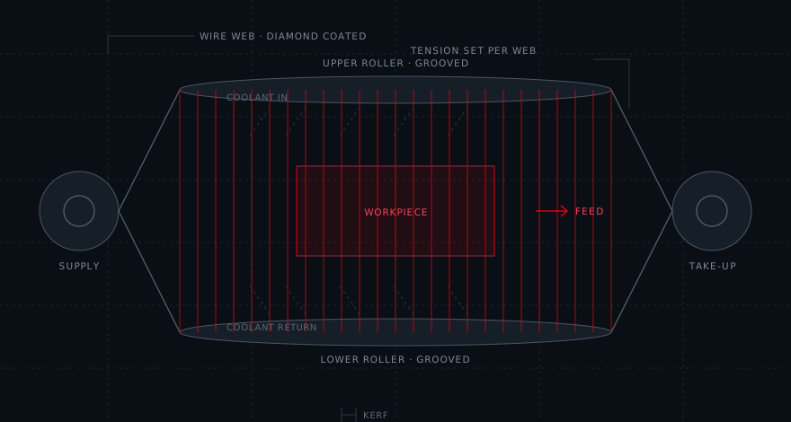
Wire diameter and abrasive size set the kerf and the depth of the damage layer that lapping must remove. Both follow the material, not stock convenience.
Coolant and debris
Flow, filtration and temperature carry heat out of the kerf. Insufficient filtration shows up as surface damage on the wafer, never as a coolant problem on the gauge.
Mounting and alignment
How the ingot is fixed and aligned decides whether the offcut measured on the X-ray diffractometer survives to the finished wafer.
Four key control points
Orientation before slicing
X-ray orientation verification before slicing, thickness-uniformity control across the batch, coolant, filtration, cleaning and contamination control, and piece-by-piece measurement before packaging. Each stage is gate-checked to prevent defects from reaching customers' lines.
Thickness across the batch
Feed rate and wire tension are held through the cut so thickness does not drift from the first slice to the last. The ±3 μm we quote is a batch figure, not a best-case piece.
Cooling and cleaning
Filtration, temperature and the cleaning step after lapping. Residue left on the surface becomes a coating defect at the customer step, long after it left our plant.
Measurement before packing
Thickness, TTV, flatness, roughness and — for optical grades — transmission, measured piece by piece and recorded against the batch number.
From boule to finished wafer — nine controlled steps
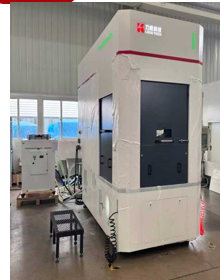
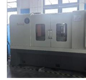
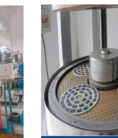
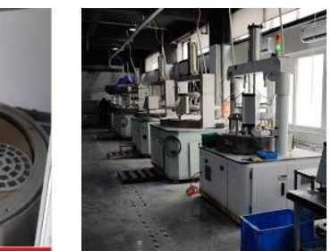
Crystal growth, head/tail cropping, OD grinding, orientation inspection, multi-wire slicing, lapping, beveling, polishing, and inspection & packaging — each step has a designated owner and quality records, ensuring full traceability.

| Property | Method | Typical value |
|---|---|---|
| Thickness | Contact micrometer, 5 points | ±3 μm (sapphire) |
| TTV / bow / warp | Capacitive or optical flatness gauge | Agreed per order |
| Flatness | Optical flat / interferometer | ≤ 0.02 mm (ceramic) |
| Surface roughness | Profilometer, Ra | ≤ 0.3 μm polished |
| Orientation | X-ray diffraction | ±2° (sapphire C-plane) |
| Transmission | Spectrophotometer | > 70 % @ 355 & 1,064 nm |
| Visual | 100 % under controlled lighting | Chips, scratches, stains |
Fully equipped metrology
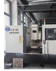
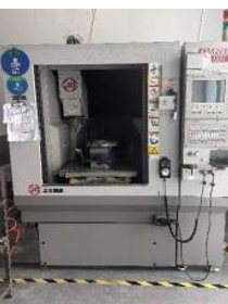
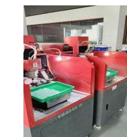
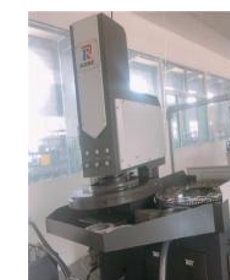
Contact micrometers, capacitive/optical flatness gauges, optical flats and interferometers, profilometers, X-ray diffractometers and spectrophotometers enable full inspection of thickness, TTV, flatness, surface roughness, crystallographic orientation, transmittance and visual appearance. Every piece is measured, data archived by batch.
- Piece-by-piece inspection, not sampling of the first wafer
- Records kept against the batch number
- Data sheet issued with the shipment
R&D and innovation
R&D closely follows customer demands and industry trends, focusing on thin-slice cutting processes, defect and warp control for 8-inch silicon carbide, and large-format sapphire PSS sheets, continuously improving process capability and yield.
- Thinner slices with tighter thickness spread
- 8-inch SiC: defect density and bow control
- Larger sapphire sheets for PSS patterning
- Trial slices as a standing offer, not a favour
| What you get | Measured how |
|---|---|
| Thickness spread | μm, across the batch |
| Flatness / TTV | μm, per wafer |
| Surface roughness | Ra |
| Orientation | Degrees, X-ray |
| Transmission | % at the agreed wavelength |
| Visual defect | Count per wafer |
News Center
Three sections — company news, technology updates and industry insights — covering production-line upgrades, process innovations and market trends. Statutory announcements are published on the Chinese site.
Sapphire substrates qualified to 6 inch
Ingot handling, orientation and polishing extended to 6-inch wafers and 310 × 310 mm sheets.
TECHNOLOGYKerf budgets tighten as wafers get thinner
Why cost per wafer, not wire price per reel, is the metric that decides a slicing process.
INDUSTRYSiC moves to 8 inch: what changes for substrate supply
Larger diameters shift the hard part from slicing to bow and defect control.
COMPANY · 2023-07Provincial delegation visits the Guangzhou Expo booth
Shandong officials toured the stand at the 18th China International SME Fair.
TECHNOLOGYOffcut tolerance decides epitaxy yield
A ±2° substrate specification is a process number, not a marketing number.
INDUSTRYMeasuring substrate quality by TTV, not by price
Two batches at the same price can differ by the cost of a whole thinning step.
System certifications and national credentials
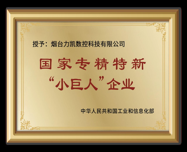
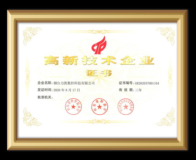
Likai Technology holds the National Specialized and Innovative "Little Giant" Enterprise, National High-Tech Enterprise and Shandong "Morning Star Factory" for Digital Economy credentials, and is certified to ISO 9001, ISO 14001, ISO 45001 and GB/T 29490.

ISO 9001 · ISO 14001 · ISO 45001 · GB/T 29490 · National High-Tech Enterprise
Ask for the measurement, not the brochure.
Send the drawing and the inspection criteria; we reply with the values we can hold in routine production, and with what we cannot.