Applications
Different applications prioritize different substrate properties: optoelectronics values transmittance and surface quality, while power devices value thermal conductivity and crystal quality. We tailor solutions for each field and use key metrics as acceptance criteria.
LED & optoelectronics
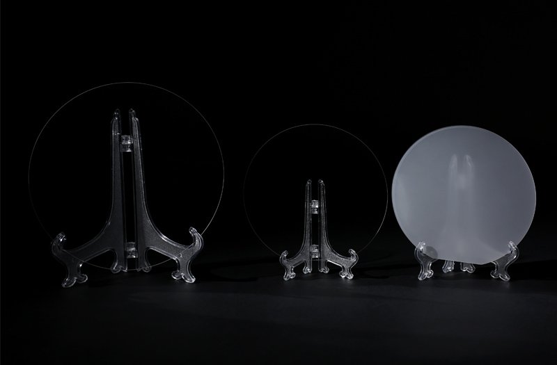
C-plane sapphire wafers and 310 × 310 mm patterned sapphire substrate (PSS) squares with an orientation tolerance of ±2° and surface roughness Ra ≤ 0.3 μm, providing flat, low-defect substrates for LED epitaxial growth.
- C-plane (0001) wafers, 2 in to 6 in
- Ra ≤ 0.3 μm and offcut within ±2°
- PSS-ready sheets in 310 × 310 mm
Power electronics
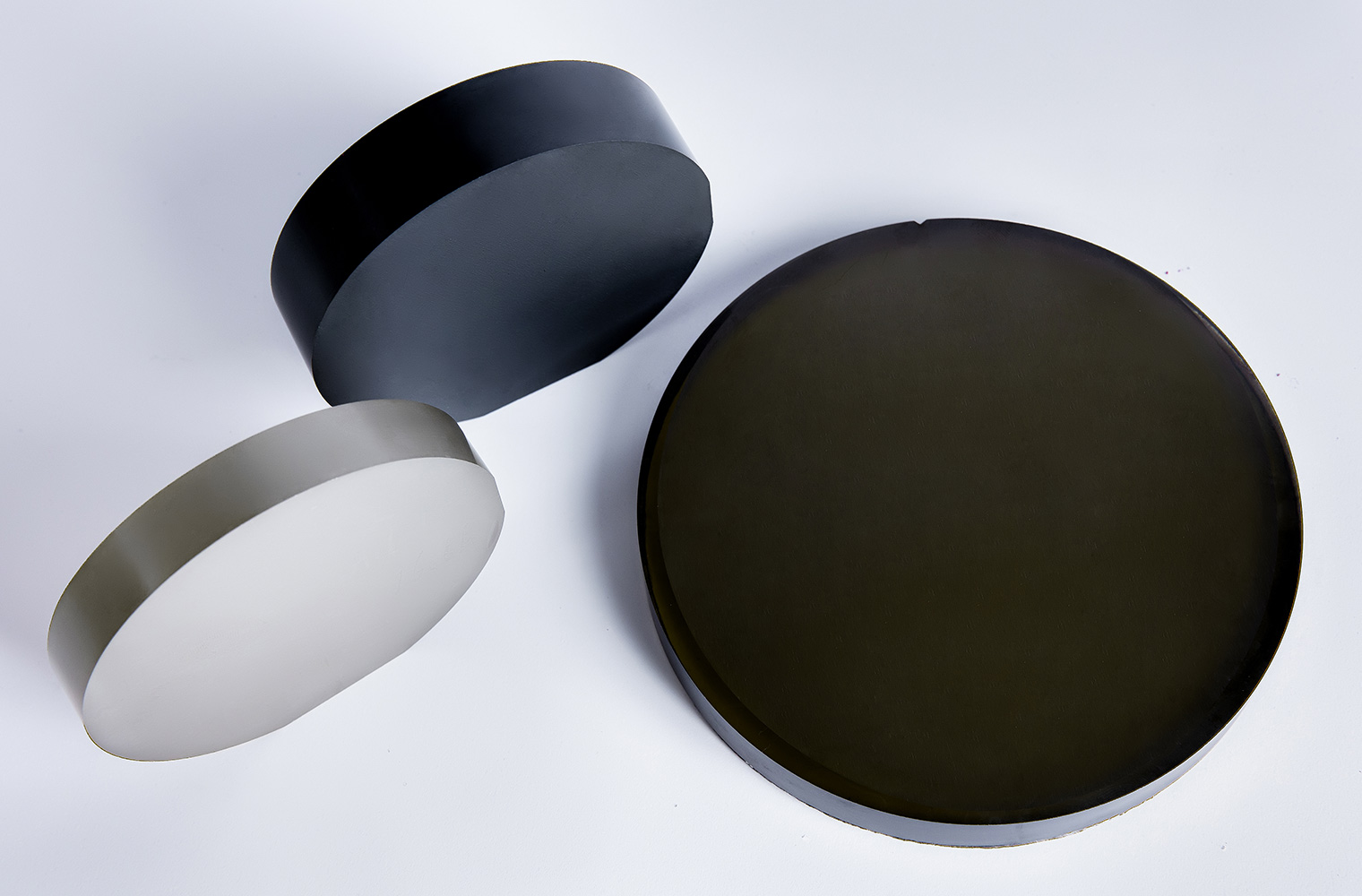
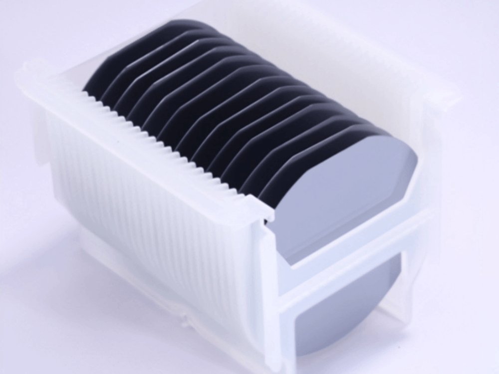
6/8-inch conductive SiC substrates for power devices such as MOSFETs and Schottky diodes; semi-insulating substrates for RF and HEMT devices. TTV and warp are tightly controlled to protect yield through wafer thinning and bonding.
- 6 in / 8 in, n-type and semi-insulating
- 350 / 500 μm, TTV and bow agreed per order
- Trial slices before a volume commitment
Consumer electronics & wearables
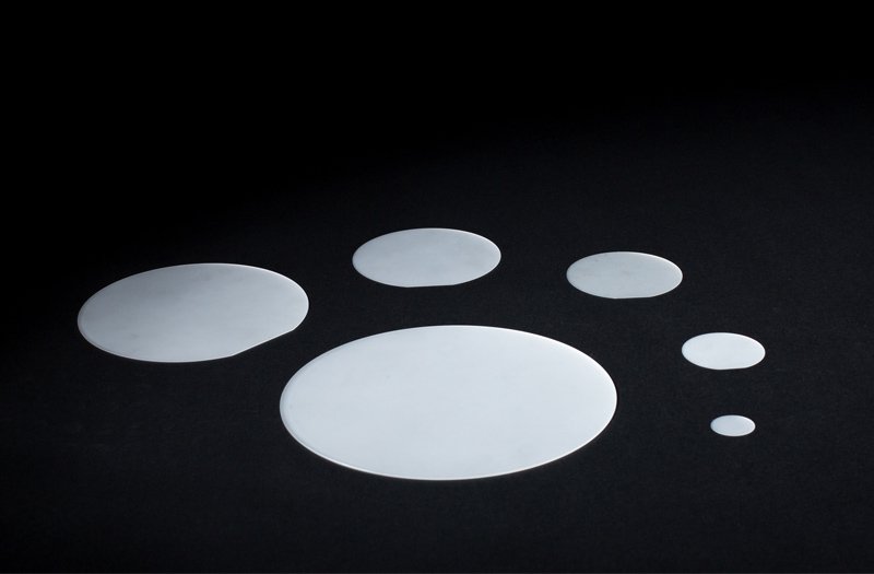
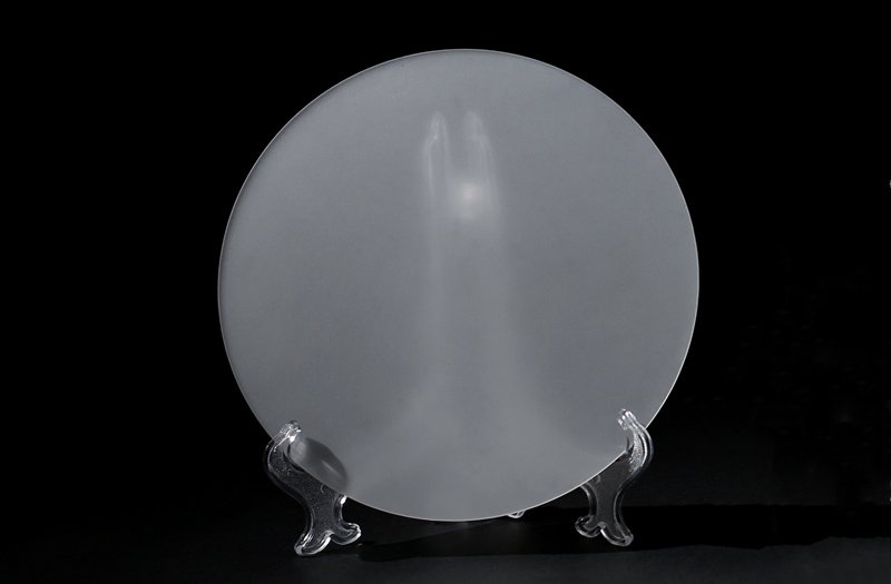
Sapphire covers, lens windows and fingerprint-sensor covers thinned to 300–700 μm, double-side polished and 100% visually inspected. Their high hardness and scratch resistance make them ideal for smartwatches, phone lenses and other consumer products.
- Thinned to 300–700 μm on request
- Edge profiling to avoid handling chips
- Double-side polish, visual inspection
Optics & ceramics
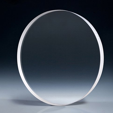
JGS-series quartz windows and alumina ceramic components. Quartz products meet high-transmittance and low-wavefront-distortion requirements; ceramics achieve flatness ≤0.02 mm. Both are manufactured per drawing, suited to precision instruments and inspection equipment.
- JGS1 / JGS2 / JGS3 quartz, up to 310 × 310 mm
- Alumina 95 % / 99 %, flat within 0.02 mm
- Chamfers, holes and steps machined before polishing
Material → application
Common pairings only; combinations not listed here are produced every month.
| Material | Application | Acceptance criterion |
|---|---|---|
| Sapphire | LED substrates, PSS sheets | Offcut and Ra |
| Sapphire | Watch covers, camera windows | Edge chips, cosmetic defect |
| Silicon carbide | MOSFETs, Schottky diodes | TTV, bow, surface finish |
| Silicon | Device development, carriers | Thickness and orientation |
| Fused quartz | Instrument windows, inspection | Transmission, flatness |
| Alumina ceramic | Substrates, wear plates | Flatness, thickness |
What leaves the plant
Five material families, each with its own failure mode and inspection criteria
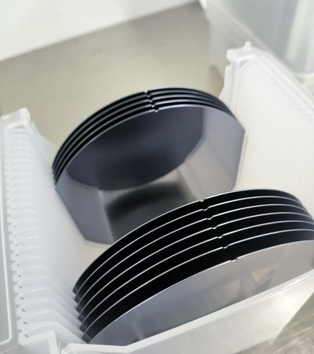
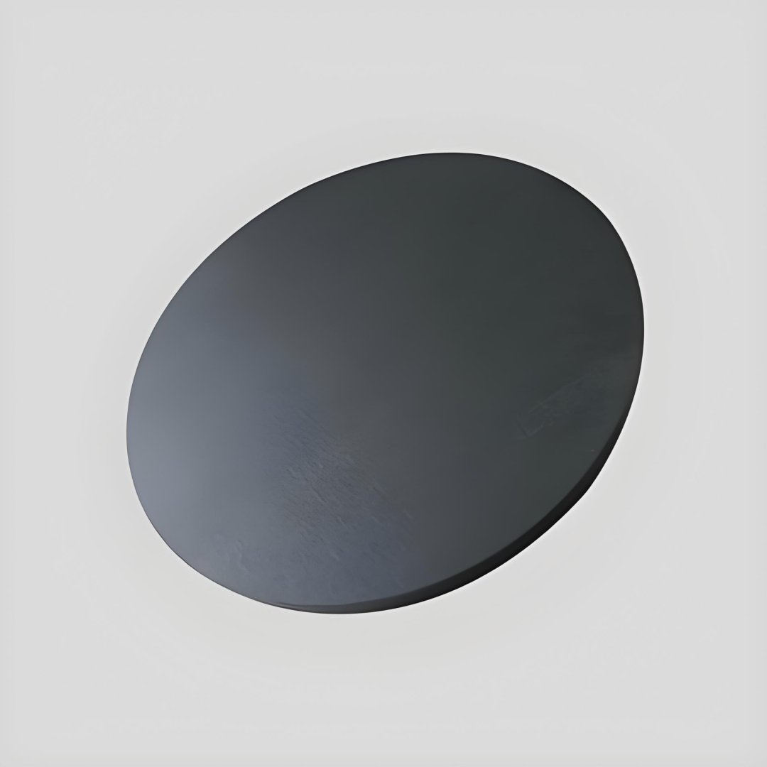
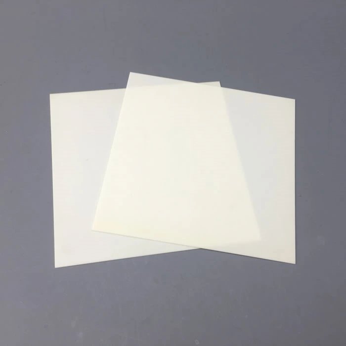
Send a drawing, get a specification.
Material, dimensions, thickness, tolerance and quantity are enough to start; trial slices are quoted separately.