
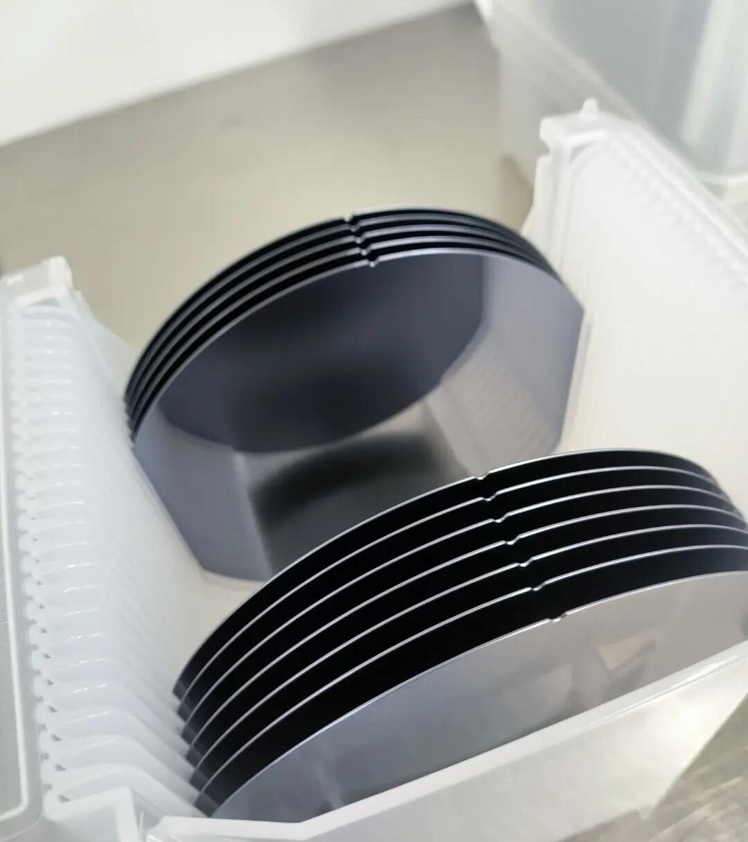
Moving 4H-SiC from 6 to 8 inch does not make slicing easier — it makes everything after slicing less forgiving. A wafer that bows by the same absolute amount spans a larger diameter, and downstream lithography sees it.
Thickness also comes under pressure: devices want thinner drift layers, so the substrate carries more of the mechanical duty while the specification asks it to be flatter and cheaper per square centimetre.
For a substrate supplier this means the value moves into metrology and process control: bow, warp, TTV and defect maps reported per wafer rather than per batch. The saw is necessary, not sufficient.
We quote SiC with TTV, bow and warp agreed per order for exactly this reason — a single published number for an 8-inch wafer would be either optimistic or useless.
Back to news