 01 / SAPPHIRE
Sapphire
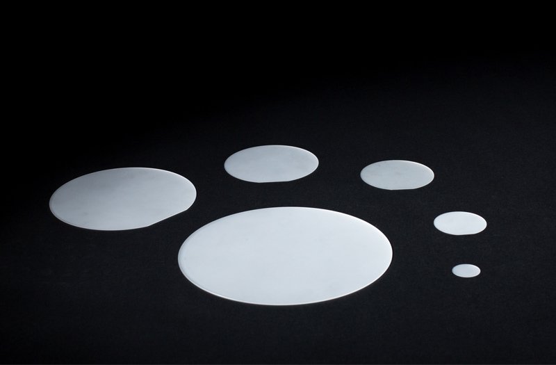
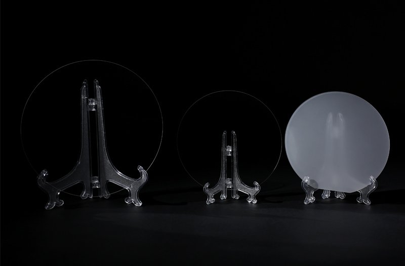
Sapphire ingots, substrates, polished wafers and 310 × 310 mm sheets for LED substrates and optical windows.
Purity> 5N
Thickness700 / 1,000 μm
Tolerance±3 μm
Yantai Likai Semiconductor Technology Co., Ltd. specializes in precision slicing and wafer processing of semiconductor materials, including sapphire, silicon carbide, monocrystalline silicon, fused quartz and alumina ceramics. With fully in-house capabilities spanning crystal growth, slicing, lapping, polishing and inspection, every piece is inspected before shipment, delivering high-precision, high-reliability substrates and wafers to customers worldwide.
The portfolio covers five major material families: sapphire, silicon carbide, monocrystalline silicon, fused quartz and alumina ceramics. From crystal growth, precision slicing, lapping and polishing to inspection and packaging, every step is performed in the same facility, enabling closed-loop quality control from material to finished product.
01 / SAPPHIRE
Sapphire ingots, substrates, polished wafers and 310 × 310 mm sheets for LED substrates and optical windows.
 02 / SILICON CARBIDE
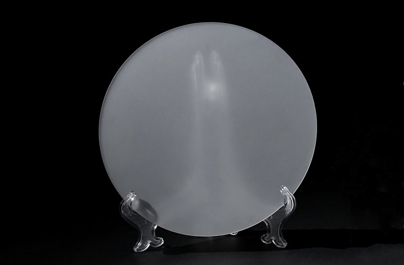
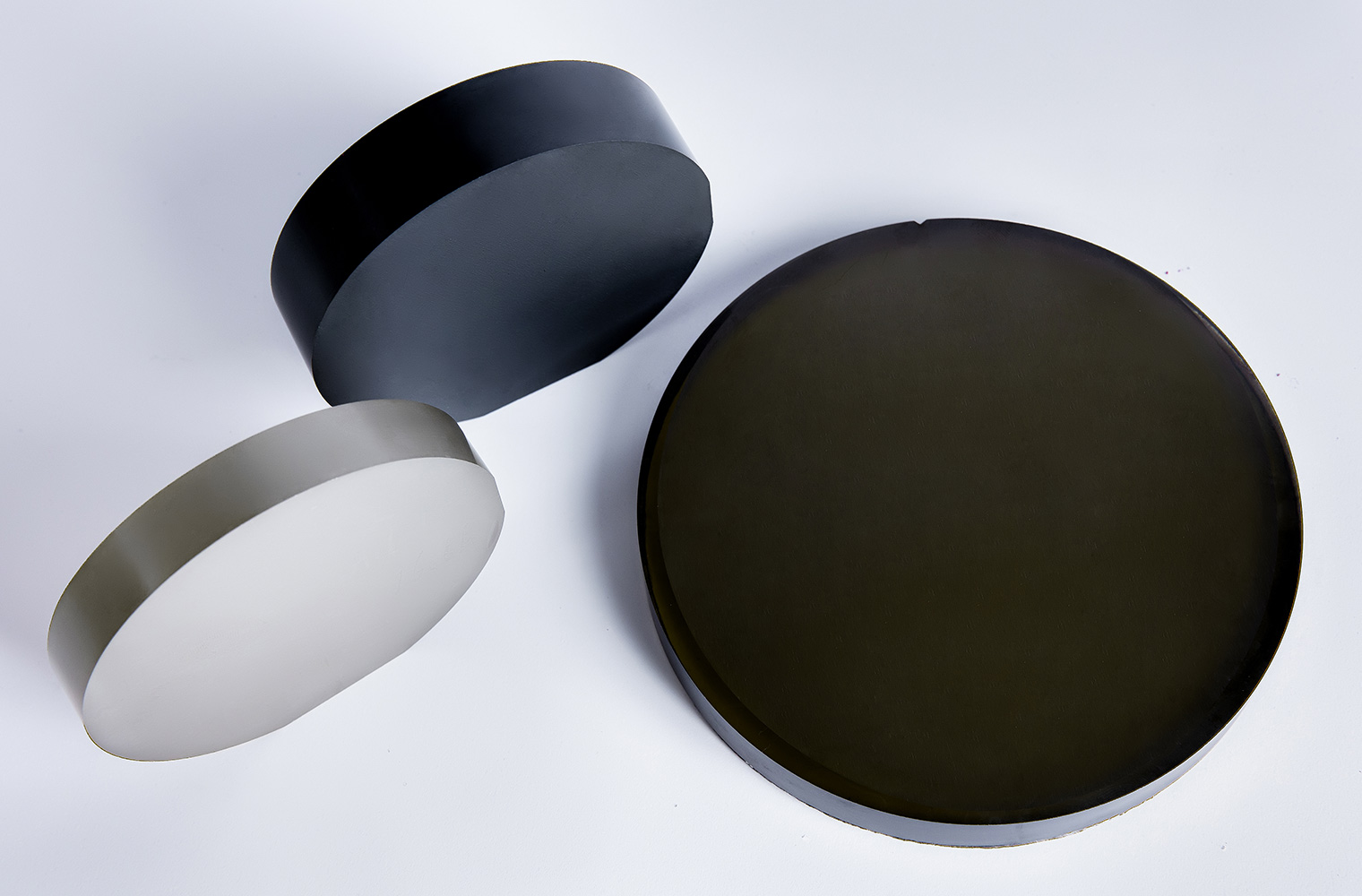
SiC substrates in 6 and 8 inch: n-type for power devices, semi-insulating for RF and HEMT.
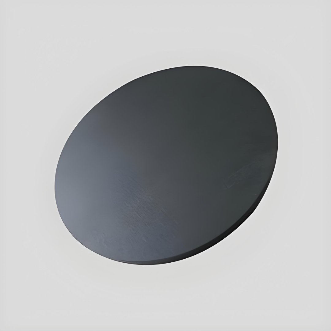 03 / SILICON
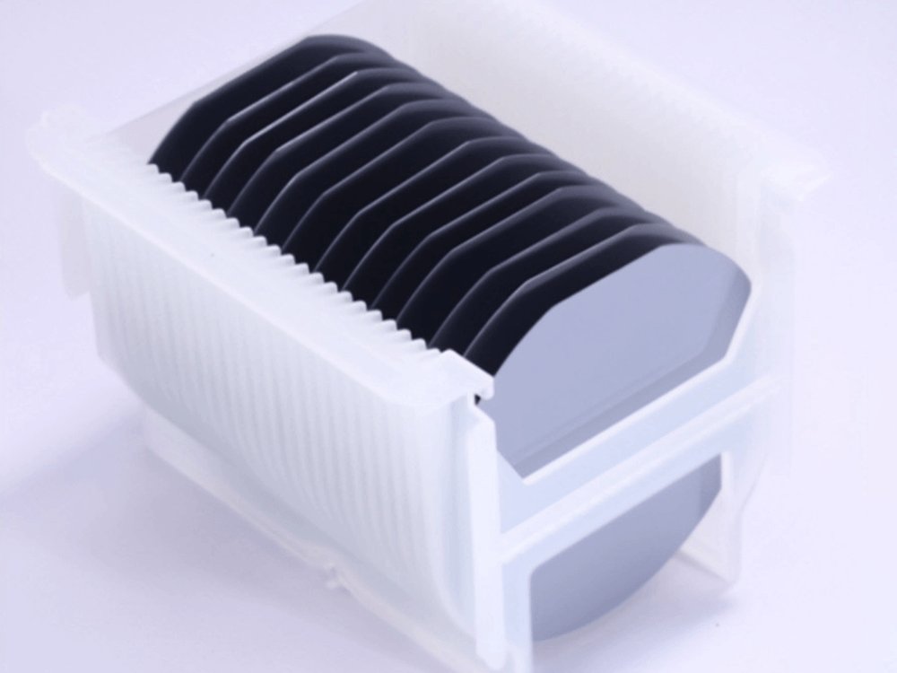
Prime and test-grade silicon wafers for device development, carrier plates and process trials.
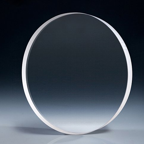 04 / FUSED QUARTZ
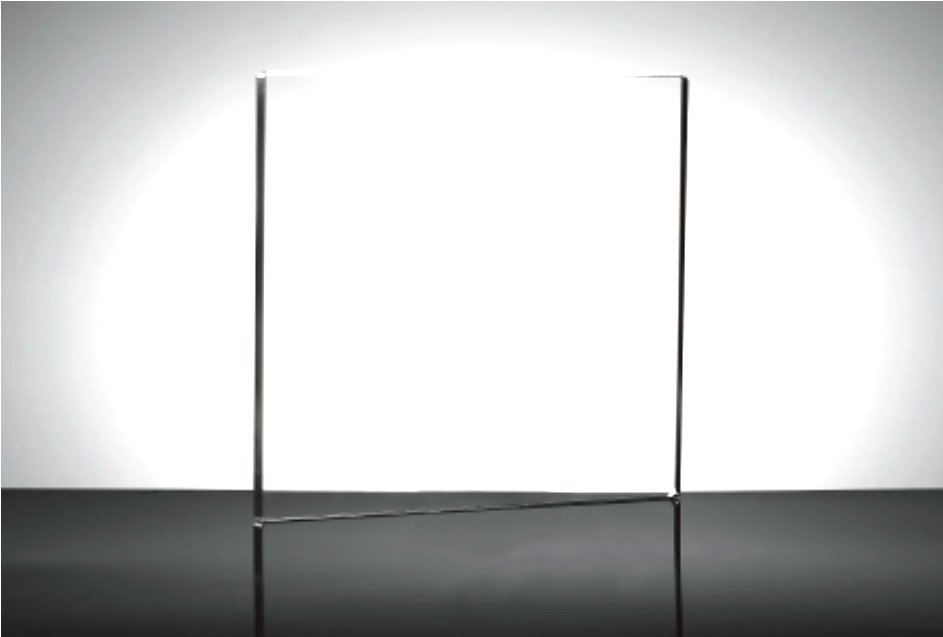
JGS1 / JGS2 / JGS3 fused quartz slides, windows and discs where transmission matters most.
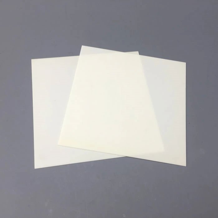 05 / ALUMINA CERAMIC
95 % and 99 % alumina substrates and wear parts, sliced and lapped to the thickness on your drawing.
Beyond standard products, the company accepts custom slicing of GaAs, GaN, glass, piezoelectric ceramics and non-standard geometries. Provide drawings and target tolerances for evaluation; new materials can be validated by sample slicing before mass production.
Send a drawingLeveraging advanced processes such as multi-wire diamond slicing, every product passes through nine controlled steps: crystal growth, head/tail cropping, OD grinding, orientation inspection, multi-wire slicing, lapping, beveling, polishing, and final inspection & packaging. Quality records are kept at every step to ensure consistent thickness, flatness and surface quality.
Kyropoulos for sapphire, PVT for silicon carbide — defect levels are set here.
Diamond saw removes the ends and shoulders; the usable body is logged with an ID.
Outer diameter ground to nominal, reference flat or notch cut in the same setup.
X-ray diffraction confirms the C-plane or the <100> face before any cut.
Diamond wire cuts the whole boule in one pass; tension and feed set kerf and damage.
Both faces lapped flat to remove saw damage and bring thickness into range.
Edges rounded to prevent handling chips, profile held within the drawing tolerance.
Double-side chemical-mechanical polishing to final thickness and roughness.
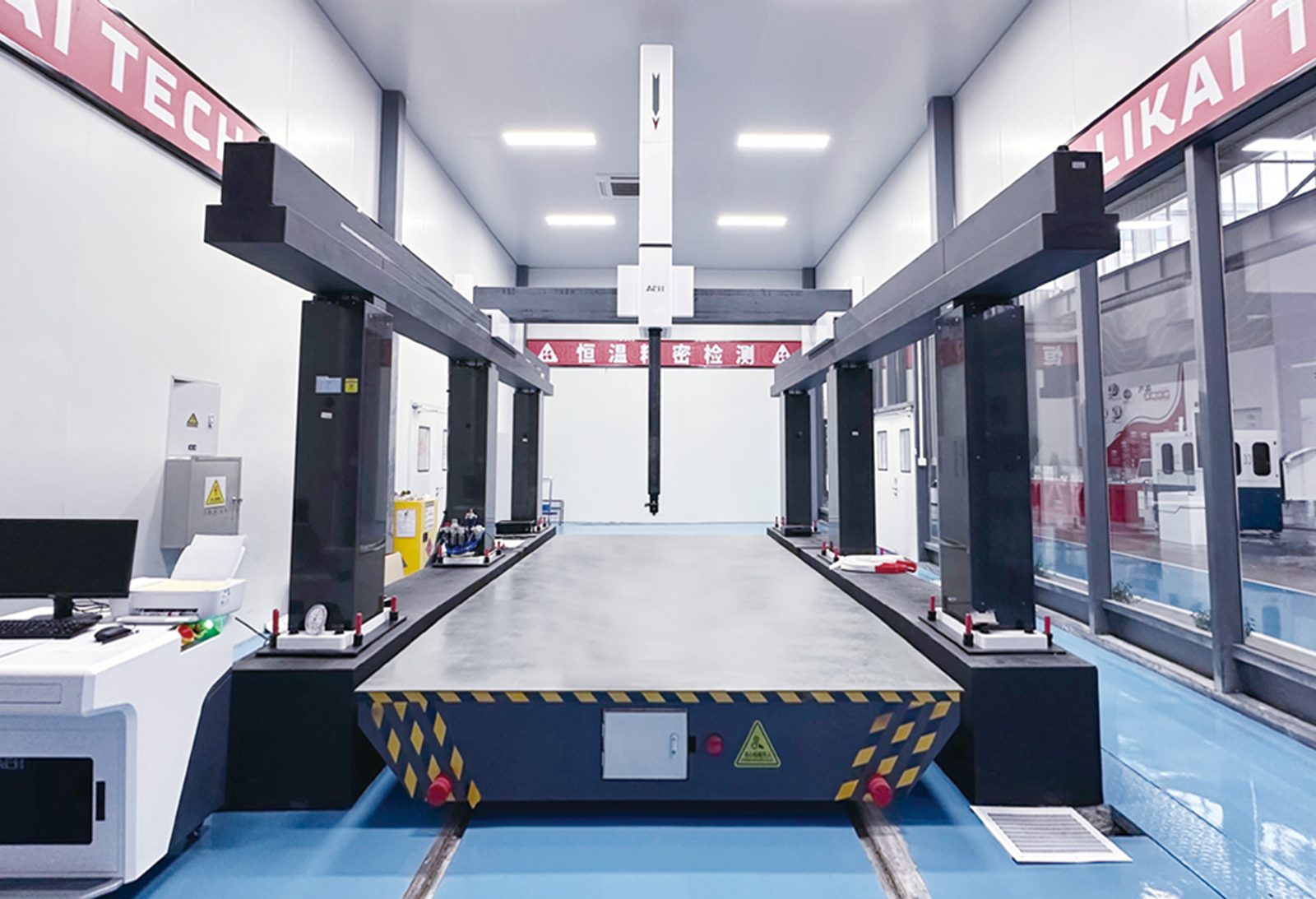
Thickness, TTV, flatness, roughness and transmission measured piece by piece, then packed in a cleanroom.
Crystallographic orientation is verified by X-ray diffraction before slicing to eliminate orientation errors. Finished products are inspected piece by piece for thickness, TTV, flatness, roughness and transmittance, with data archived by batch number. Wafers are double-layer packaged under controlled clean-room conditions, with a certificate of conformance and inspection report enclosed.
C-axis offcut and reference flat are verified on every ingot before slicing.
Thickness, TTV, flatness, roughness and transmission are recorded against the batch number.
Double-bagged in a controlled area, with a certificate of conformance in the box.
Our products serve LED & optoelectronics, power electronics, consumer electronics & wearables, and optics & ceramics, providing downstream customers with stable, reliable substrates and wafers.
Patterned sapphire substrates and C-plane wafers.
SiC substrates for MOSFETs and Schottky diodes.
Sapphire covers for watch crystals, camera lenses and fingerprint sensors.
Quartz windows and alumina ceramic parts for instruments.
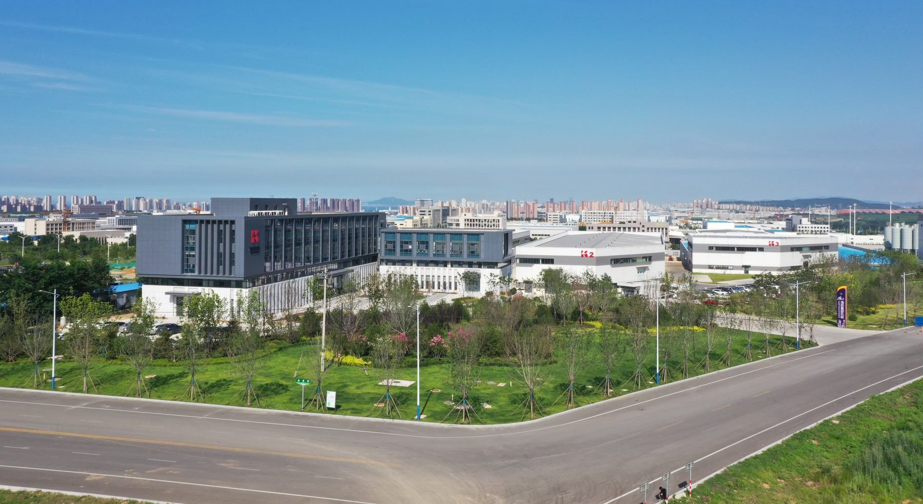
Yantai Likai Semiconductor Technology Co., Ltd. ("Likai Semiconductor") is a wholly owned subsidiary of Yantai Likai CNC Technology Co., Ltd. ("Likai Technology"), extending the group's cutting technology into semiconductor materials.
Specializing in precision slicing of semiconductor materials, the company covers sapphire, silicon carbide, monocrystalline silicon, quartz glass and alumina ceramics, and also offers customized slicing of gallium arsenide and gallium nitride. Its complete in-house line — from crystal growth through slicing, lapping, polishing and inspection — runs nine controlled processes. Backed by diamond-wire multi-wire cutting and X-ray crystal-orientation inspection, it achieves sapphire thickness tolerance ±3 μm and surface roughness Ra ≤ 0.3 μm, with every piece inspected and data archived by batch number. Products serve LED and optoelectronics, power electronics, consumer electronics, optics and ceramics, as the company works to become a professional service provider in precision slicing of semiconductor materials worldwide.
2018, Yantai → Likai Technology · National “Little Giant” Enterprise
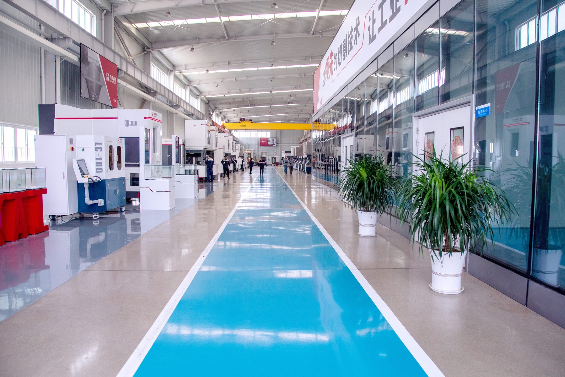
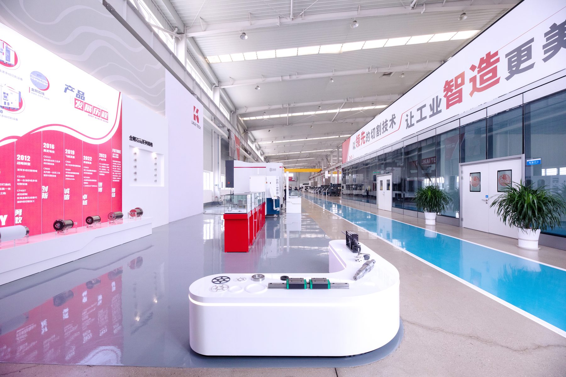
Yantai Likai Numerical Control Technology Co., Ltd. ("Likai Technology"), established in June 2018, is a high-tech enterprise covering the entire cutting technology industry chain — equipment, diamond wire and multi-wire cutting services. It is a national "Little Giant" enterprise specializing in niche and innovative products, a "Double Soft" certified enterprise, and an industrial enterprise intellectual property application pilot enterprise recognized by China's Ministry of Industry and Information Technology, specializing in the R&D, production and sales of hard and brittle material cutting equipment.
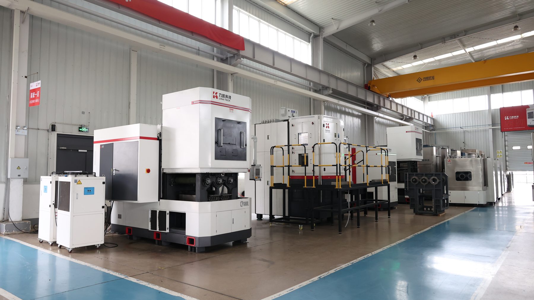
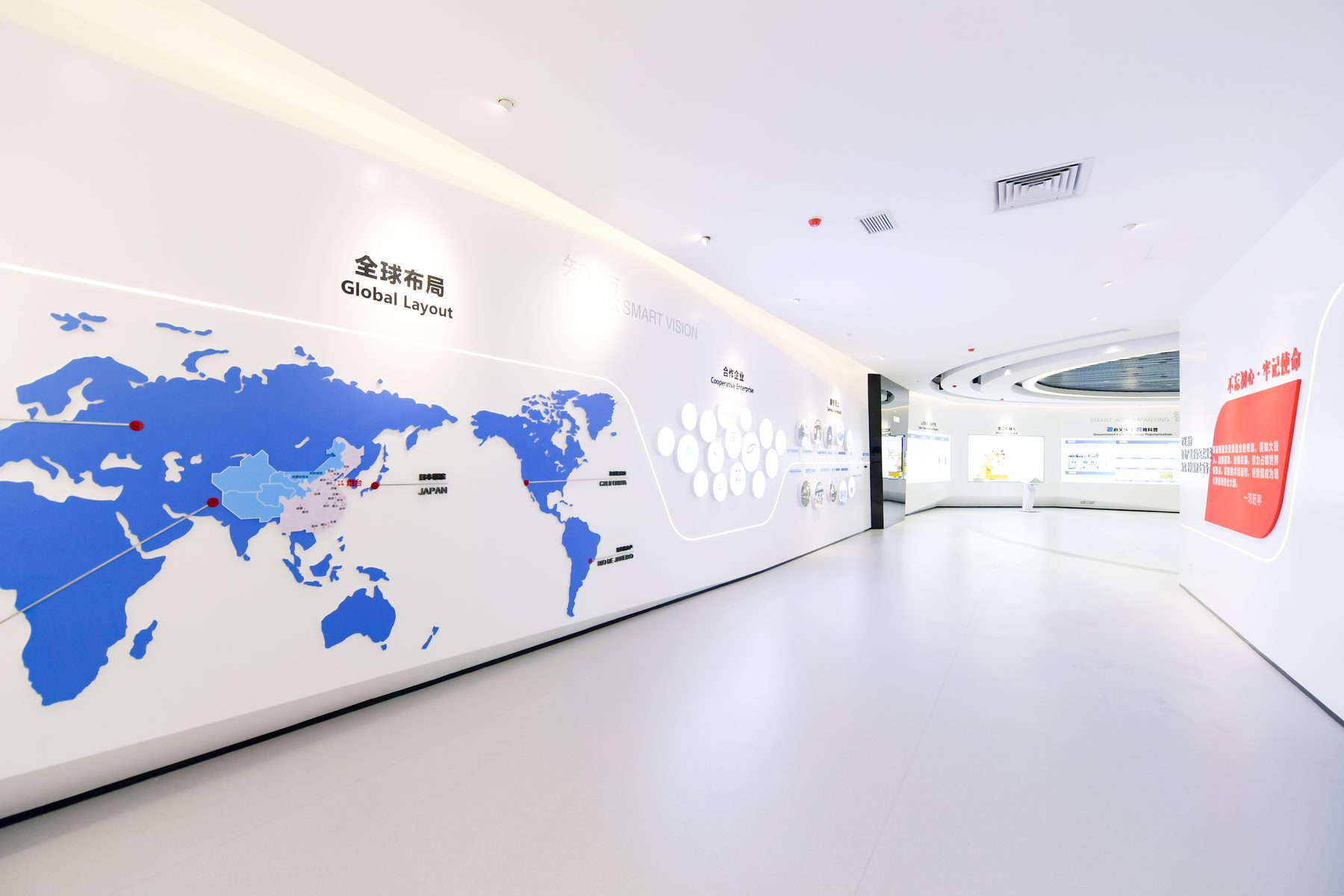
The company holds ISO 9001, ISO 14001, ISO 45001 and GB/T 29490 management system certifications, as well as EU CE and UL certification. Its core products include multi-wire cutting equipment, laser cutting equipment and chamfering equipment, which are widely used in advanced hard and brittle materials such as metal materials, sapphire and semiconductor materials. These products are exported to more than ten countries and regions, including the United States, Japan, South Korea, the United Kingdom, Singapore, Brazil and India, providing comprehensive support in equipment, processes and R&D for Likai Semiconductor.
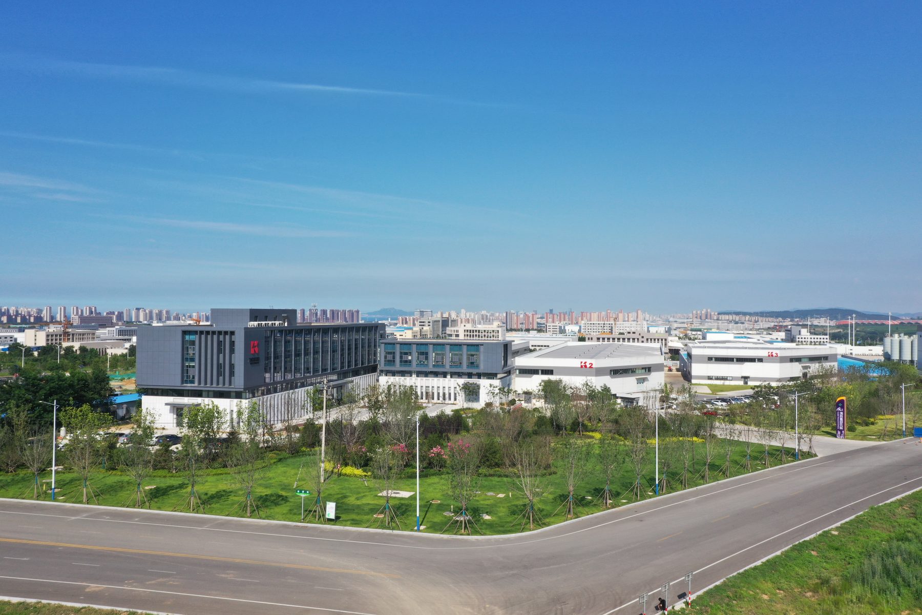
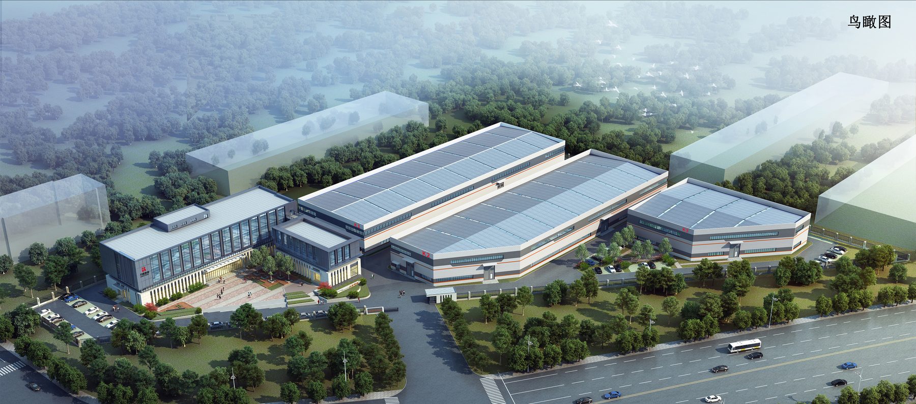
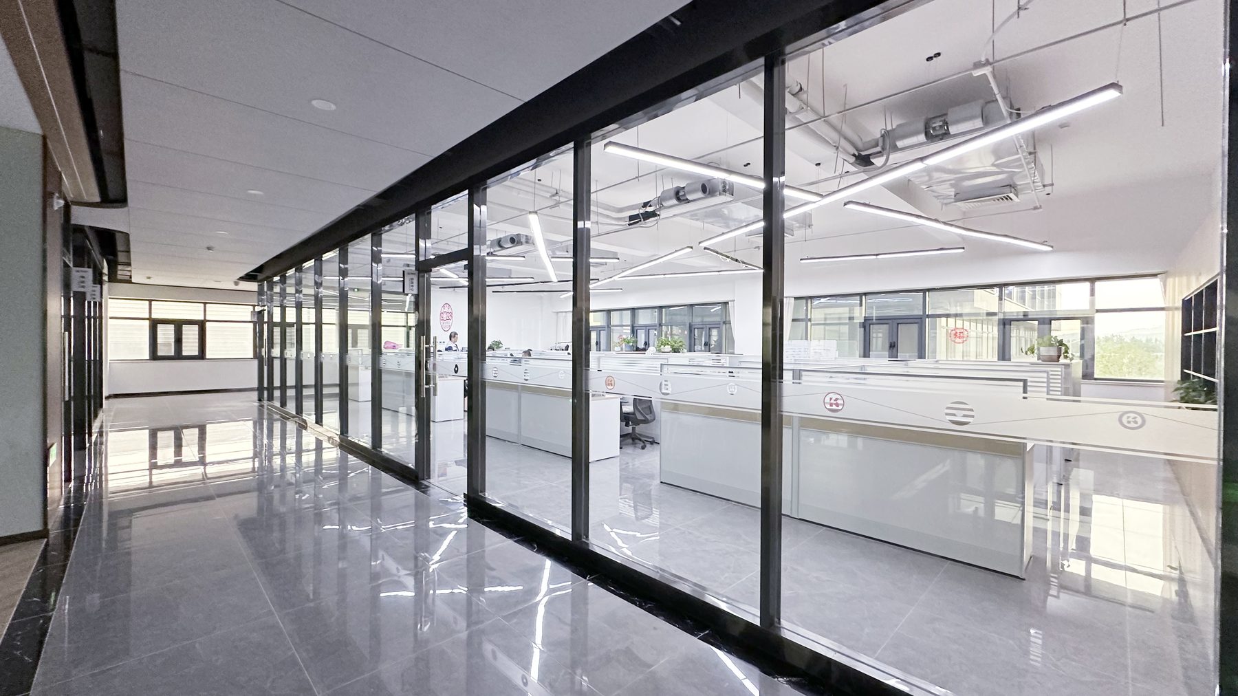
Crystal growth, slicing, lapping, polishing and inspection are all performed at the same facility in Yantai, ensuring efficient process flow and closed-loop quality control, with full traceability of quality records at every stage.
Send the material, dimensions, thickness and quantity; we reply with a feasible specification and a lead time — and say so plainly when it is out of range.